Incorrect output behavior can occur when large negative input voltages in comparators violate the input common-mode voltage range. In cases where it’s not possible to avoid a negative input voltage, it’s important to protect the input pins of the comparator and prevent a phenomenon called phase reversal, also known as phase inversion, from occurring.
In this article, I’ll explore the causes and effects of negative input voltages in comparators, the behavior of phase reversal, and how you can protect inputs from negative voltages.
Negative input causes and effects
Negative voltages can come from many unexpected and unavoidable sources, including switching noises in DC/DC converters, AC-coupled inputs that create a bipolar voltage at the input, and ringing from inductive sources of bipolar outputs. In systems such as automotive and industrial applications, large negative inputs can also arise from ground offsets or ground shifting in which there are two different reference points that sit at different potentials; this occurs when there are split ground planes to isolate the analog circuitry from high-current switching nodes.
Manufacturers build comparators without dedicated electrostatic discharge structures to protect against large negative input voltages using a junction-isolated die process, where P-N junctions act like diodes under every node connected to the common die substrate. It’s important to maintain the connection to the common die substrate at the most negative potential tied to the GND pin. If the input pins are more negative than the GND pin – and therefore the substrate – excessive reverse currents will cause parasitic elements to appear and turn on internal parasitic N-channel P-channel N-channel transistors that take current from other internal nodes and channels. This can lead to phase reversal.
Phase reversal
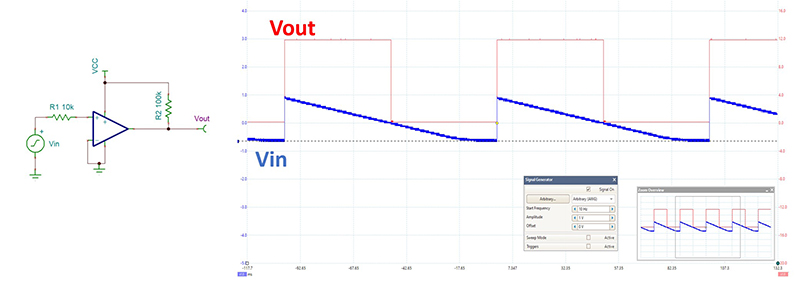
Under phase-reversal conditions, the polarity of the output incorrectly inverts. Figure 1 shows a comparator in a noninverting configuration in which the reference voltage at IN– is tied to 0 V at GND. As the input voltage goes below 0 V, the output voltage goes low as expected. As the input reaches about –570 mV, however, the output voltage inverts and goes high.

Figure 1: Phase reversal in a comparator
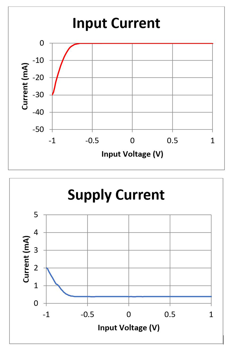
Figure 2 shows the input and supply currents of the comparator as the input sweeps below 0 V. As the input voltage increases more negatively, the reverse current increases significantly. The supply current also increases because of the extra P-N junctions that are now turned on and conducting.

Figure 2: Input current and supply current caused by negative input
How to protect inputs from negative voltages
In order to protect the comparator’s inputs and prevent phase reversal, you must first analyze the device’s minimum input voltage and maximum input current. Figure 3 shows the LM2903B’s absolute maximum ratings table, which states that the minimum input voltage is –0.3 V and the maximum input current is 50 mA. These specifications make it impossible to define an operation with a negative input voltage more than 0.3 V, because it violates the input voltage specification and does not guarantee proper operation. The maximum current that the comparator can withstand is 50 mA: any amount of current larger than that can damage the device. And while limiting the current right under 50 mA will not damage the device, phase reversal may still occur, which means that you must limit the current to a value much lower than 50 mA for proper comparator operation.
|
Min |
Max |
UNIT |
| VCC |
Non-B Versions |
-0.3 |
36 |
V |
| B Versions Only |
-36 |
38 |
| VID |
Non-B Versions |
-38 |
36 |
V |
| B Versions Only |
-0.3 |
38 |
| VI |
Non-B Versions |
36 |
V |
| B Versions Only |
|
38 |
| IIK |
|
-50 |
mA |
| VO |
Non-B Versions |
|
36 |
V |
| B Versions Only |
|
38 |
| IO |
Non-B Versions |
|
20 |
mA |
| B Versions Only |
|
25 |
| ISC Duration of output short to ground |
Unlimited |
|
| TJ Operating virtual-junction temperature |
|
150 |
°C |
| Tstg Storage temperature |
-65 |
150 |
°C |
Figure 3: Absolute maximum ratings table for the LM2903B
I don’t recommend operating these devices outside of their absolute maximum limits. In cases where you cannot avoid doing so, using a series current-limiting resistor along with an external Schottky diode, placed at the input pin to GND, can help limit the voltage and current to a safe level so that the body diode does not start to conduct, as shown in Figure 4.

Figure 4: Current-limiting resistor with a Schottky diode at the input of the comparator circuit
A general rule of thumb is to select a resistor that is 1 k? per voltage of the maximum negative voltage so that the current is limited to 1 mA or less. For example, if the maximum negative input voltage is –2 V, the resistor must be at least 2 k? or larger. Following this rule will ensure that the input current is well within the absolute maximum specifications and prevent damage to the comparator.
The Schottky diode has a lower forward voltage than the body diode and will start to conduct around 0.2 V before the body diode starts to conduct around 0.4 V. This external diode, along with keeping the current to 1 mA or less, will help make sure that the negative input voltage signal clamps below 0.3 V and thus avoids phase reversal.
Another option is to use a comparator that has better protections against phase reversal, such as the TLV1701 high-voltage micropower comparator. Figure 5 shows its absolute maximum ratings. The minimum input voltage is 0.5 V below VS– and the maximum input current is 10 mA.
|
MIN |
MAX |
UNIT |
| Supply voltage |
|
+40 (±20) |
V |
| Signal input pins |
Voltage |
(VS-) - 0.5 |
(VS+) + 0.5 |
V |
| Current |
|
±10 |
mA |
| Output short-circuit |
Continuous |
mA |
| Operating temperature range |
-55 |
+150 |
°C |
| Junction temperature, TJ |
|
150 |
°C |
| Storage temperature, Tstg |
-65 |
+150 |
°C |
Figure 5: Absolute maximum ratings table for the TLV1701
Figure 6 shows the TLV1701 in a noninverting configuration with its inverting input tied to 0 V at GND. As the input voltage goes below 0 V, the output voltage does not invert, even when the input voltage is beyond the –0.5-V limit. As the input sweeps more negatively, the input current will start to increase exponentially and go above the 10-mA maximum limit, which may damage the comparator. Therefore, adding a 10-k? resistor in series with the input helps reduce the current to a safe level.

Figure 6: The TLV1701’s output voltage with a negative input
Conclusion
When designing with comparators, it’s important to consider the effects of negative inputs and how they may cause phase reversal in the output. In many systems such as automotive and industrial applications, these large negative voltages cannot be avoided. Operation outside the recommended limits is not warrantied so it is crucial to take measures to prevent damage to the comparator and phase reversal from occurring. Using the methods mentioned in this article can help improve circuit performance and minimize unwanted output behavior that may cause issues for the downstream devices in the system.
Additional resources


