The input common-mode voltage range (commonly abbreviated as VCM or VICR) is a term that’s widely recognized in the analog world but misunderstood in the comparators world. For an amplifier, VCM is defined as the average voltage applied to both inputs. But for a comparator, it has an entirely different meaning.
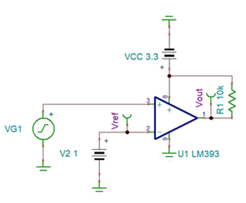
The normal operation of a comparator implies two inputs crossing, causing a change in the output. Let’s analyze the noninverting comparator configuration shown in Figure 1, with its transient behavior graphed in Figure 2.

Figure 1: Noninverting comparator configuration

Figure 2: Noninverting comparator transient behavior
In Figure 2, if the voltage at the noninverting terminal (olive green) is greater than the voltage at the inverting terminal (red), then the output (green) is high. If the inverting terminal voltage is greater than the noninverting terminal, then the output is low. A comparator’s input VCM is the switching point where the two input voltages cross one another. The voltage range of that switching point that still ensures normal operation is known as a comparator’s input VCM.
Table 1 shows the LM393’s VCM, which ranges from the negative supply, V–, to 1.5 V or 2 V below the positive supply, V+, depending on the temperature of the device.
|
Parameter
|
Test conditions
|
Min Typ Max
|
Unit
|
|
VCM
|
Common mode range
|
VS = 3 to 36 V
|
(V-) (V+) – 1.5
|
V
|
|
VS = 3 to 36 V, TA = -40°C to +85°C
|
(V-) (V+) – 2
|
V
|
Table 1: Row from LM393 datasheet table 6.7 Electrical Characteristics
If I powered this device using a 3.3-V supply at room temperature, then the input VCM of the device is between ground and 1.8 V. If the switching point moves higher than 1.8 V, the device may not function. And if one or both inputs violate VCM, improper operation may occur.
What limits the input VCM?
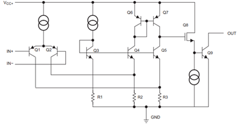
The input stage of the comparator limits the input VCM. Let’s first look at a functional block diagram from the TL331 data sheet (Figure 3). The input stage comprises a for P-channel, N-channel, P-channel (PNP) differential pair whose emitters connect to a current source. For the PNP transistor on the differential pair to conduct, there needs to be a voltage drop from the emitter to base (VEB) (for an N-channel, P-channel, N-channel configuration, this would be base to emitter [VBE]).

Figure 3: TL331 functional block diagram
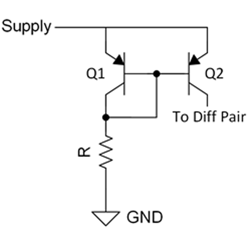
The current source is usually a current mirror, as shown in Figure 5. For the current source to work, the emitter-to-collector voltage of Q2 needs to exceed the minimum forward active voltage requirement (VEC (Sat)).

Figure 4: PNP current mirror
As the comparator input voltages increase, there is less headroom available to satisfy both the VEB turnon of the differential pair transistor and the VEC (Sat) of the current mirror transistor. When this happens, VEC begins to shrink, while VEB still holds firm. When the VEC (Sat) does not exceed on Q2, the current-producing capabilities of the current mirror significantly diminish, which is why some comparators have VCM go up to a value below the supply voltage. Other devices that have an input stage with NPN transistors specify a VCM that ranges from a value up to the positive supply.
Why a design may work even when exceeding the input VCM on the data sheet
The values for VCM on the data sheet consider performance across process, voltage and temperature (PVT). Recalling the TL331 example in Figure 4, VBE and VCE fluctuate across temperature.
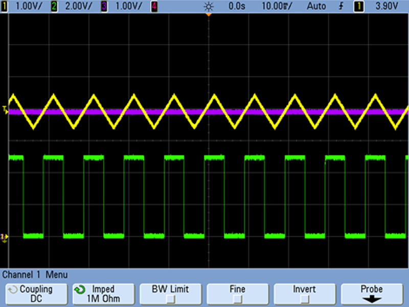
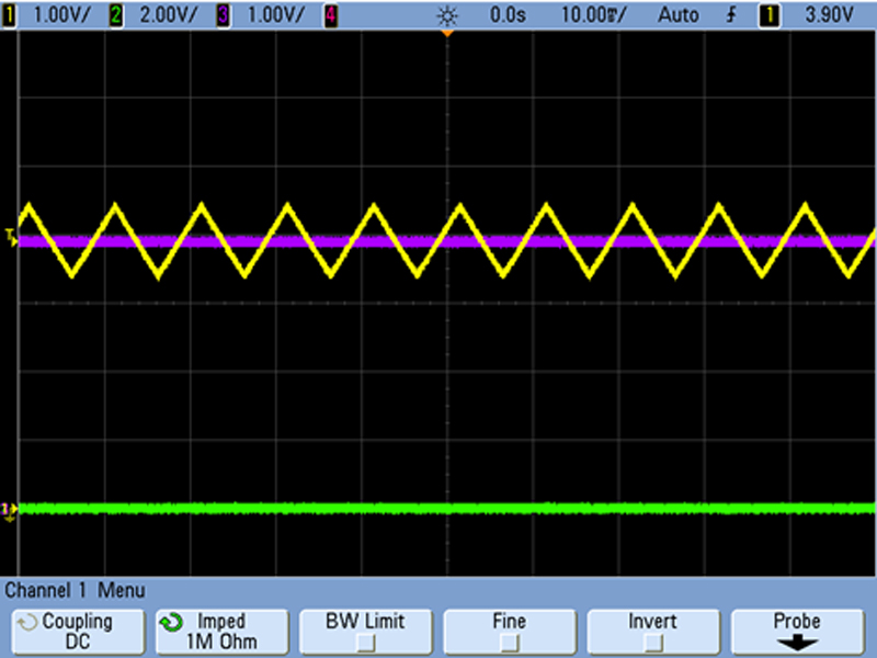
Figures 5, 6 and 7 show the performance of the LM393 in a noninverting configuration similar to Figure 1. In this case, the supply voltage is set at 5 V. A 100-Hz, 1-Vpp, 3.9-VDC ramp waveform (yellow) connects to the noninverting terminal while applying a 3.9-VDC reference signal (purple) to the inverting terminal. This is an example of an application where a switching point of 3.9 V violates VCM; with this supply, a compliant VCM is 3 V or lower.
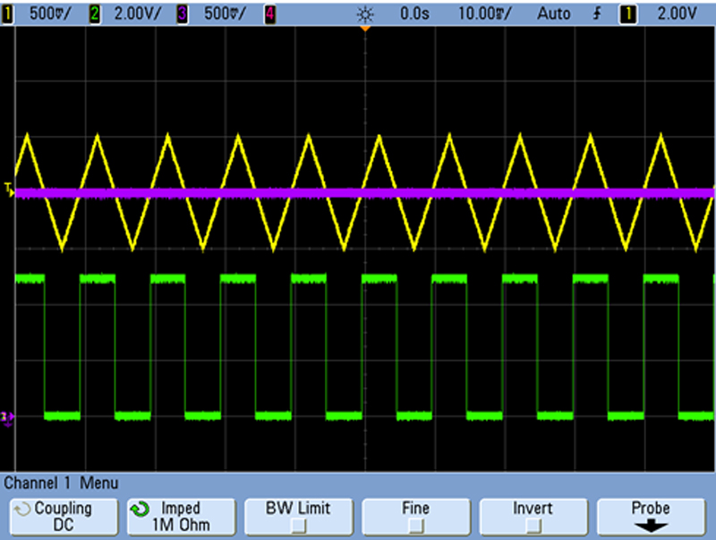
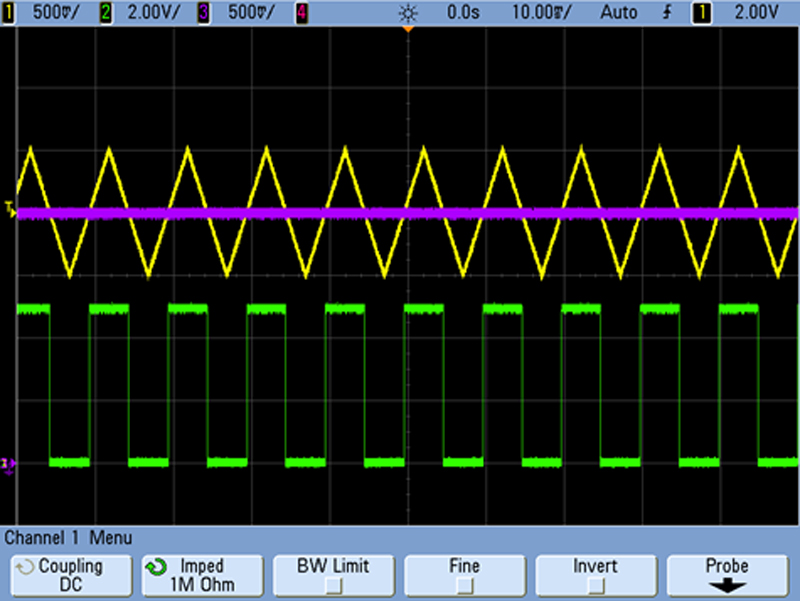
At room temperature, the comparator worked and toggled whenever it crosses 3.9 V, as shown in Figure 5. The comparator also worked when heated up, as illustrated in Figure 6. When I cooled the device down, it began to fail, as the output (green) indicates in Figure 7.

Figure 5: LM393 room temperature performance outside VCM

Figure 6: LM393 hot temperature performance outside VCM

Figure 7: LM393 cold temperature performance outside VCM
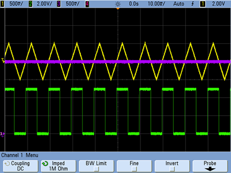
When I lowered the input voltages to ensure that the switching point was within the VCM of the device, this same device worked correctly across all temperature ranges. The ramp waveform is now at a lower DC offset of 2 V with a reference of 2 V, ensuring that the switching point remains within VCM. Figures 8, 9 and 10 show how the LM393 performs normally across temperature.

Figure 8: LM393 room temperature performance inside VCM

Figure 9: LM393 hot temperature performance inside VCM

Figure 10: LM393 cold temperature performance inside VCM
I took all of these scope captures from a single unit. If I were to test another LM393 sample, the performance outside the specified VCM range may vary. At room temperature, the VCM upper limit may differ from the tested unit. This is called process variation, where performance can vary due to lot variation or nonuniform manufacturing procedures.
The final part of this variation is voltage variation. Parts may act differently with different supply voltages. In the setup for Figures 6, 7 and 8, if the supply voltage increased to the maximum allowable 36 V, with the same VCM violation, the performance could differ. When designing a system using a comparator, it is imperative to keep the inputs within VCM to avoid these issues.
Conclusion
The input VCM can cause non-functionality of a device when either input exceeds the range. Exceeding this range causes issues with the biasing of the input stage of the comparator. Remember that one or both inputs outside the data-sheet specification is a violation of VCM. Even if the system works while violating VCM, it may not function at a different supply voltage, a different operating temperature or with a replacement integrated circuit.
When creating a system that uses a comparator, keep each of the input signals within the data-sheet specification of the input VCM in order to preserve functionality across PVT.
The third installment of this series will cover incorrect output states caused by negative inputs.
Additional resources


