The transimpedance amplifier (TIA) is one of the most common circuits in the world of precision analog circuits. The dynamic range required of a single TIA can be quite a challenge, often spanning many decades, such as picoamperes to microamperes.
Selecting a single resistor to accommodate such a wide dynamic range is a lose-lose situation, so circuit designers will often turn to an array of switches to select a few different resistor values, depending on the current level measured at the time. The switch on-resistance (RON), drift and nonlinearity do play a significant role in TIA accuracy, however, particularly at lower feedback resistor values.

Maximize accuracy in your transimpedance amplifier design

TI’s OPA3S328 is a dual operational amplifier with integrated switches for transimpedance applications. It includes two wide-bandwidth (40 MHz) low-input bias current precision amplifiers with a multiplexer to select the different gains, and a second set of switches for Kelvin sensing. In this article, I’ll illustrate the advantages of Kelvin sense switching connections over traditional switched-gain TIA circuits.
This is the second installment in a four-part series discussing how to increase system accuracy and efficiency with operational amplifiers built on TI’s new, proprietary complementary metal-oxide semiconductor precision process technology.
The programmable-gain TIA
It is possible to implement a TIA by cascading a single-gain TIA with a second programmable gain amplifier (PGA) stage. However, a better approach is to incorporate the programmable gain and TIA into a single stage. This approach provides a significant advantage from a noise performance perspective, since the sensor signal is gained on the first transimpedance stage, resulting in lower total output noise.
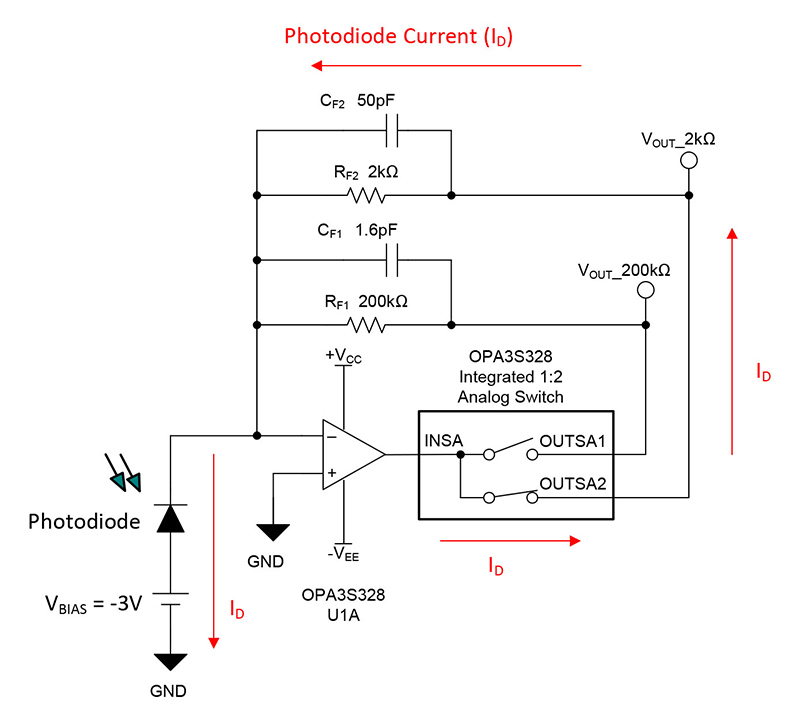
Figure 1 shows a programmable-gain TIA using the OPA3S328. The integrated 1-to-2 analog switch selects the different transimpedance feedback resistors.

Figure 1: Switched-gain TIA
The feedback resistor (RF) determines the gain of the transimpedance operational amplifier and converts the photodiode current (ID) to a voltage (VOUT) using Ohm’s law, VOUT = IDRF. For an accurate transimpedance current-to-voltage conversion, the amplifier’s input bias current and input offset voltage must be small. The OPA3S328 offers a low offset voltage of ±10 μV and a low-input bias current of ±0.2 pA. The gain resistors are typically decades apart to provide optimal resolution for different ranges of current.
Switch characteristics
Consider the electrical characteristics of the switches when designing the switched-gain TIA. The capacitances and resistances of the switch will affect the bandwidth and stability of the circuit. Furthermore, the RON of the switch can be a source of gain error.
The OPA3S328 incorporates two sets of low-leakage, low-capacitance switches useful for different circuit configurations, including programmable-gain transimpedance applications. The quad flat no-lead package version of the OPA3S328 features switch A in a 1-to-2 matrix configuration and switch B in a 1-to-3 matrix configuration.
Table 1 shows the critical data-sheet switch parameters.
|
Parameter
|
Test condition
|
Minimum
|
Typical
|
Maximum
|
Unit
|
|
CIN
|
Switch open, INSA/B = 2.5 V
|
|
3
|
|
pF
|
|
COUT
|
Switch open, OUTSA/B/1/2/3 = 2.5 V
|
|
0.7
|
|
pF
|
|
CINOUT
|
Switch closed, INSA/B = OUTSA/B/1/2/3 = 2.5 V
|
|
6
|
|
pF
|
|
RON
|
Switch closed, V+ = 5 V, INSA/B = 2.5 V
|
|
84
|
125
|
?
|
Table 1: OPA3S328 switch characteristics
CIN and COUT represent the open switch parasitic switch capacitance, while CINOUT represents the total switch capacitance while the switch is closed. RON is the switch series resistance when the switch is closed. Figure 2 shows a simplified switch model.

Figure 2: Simplified switch model for the OPA3S328
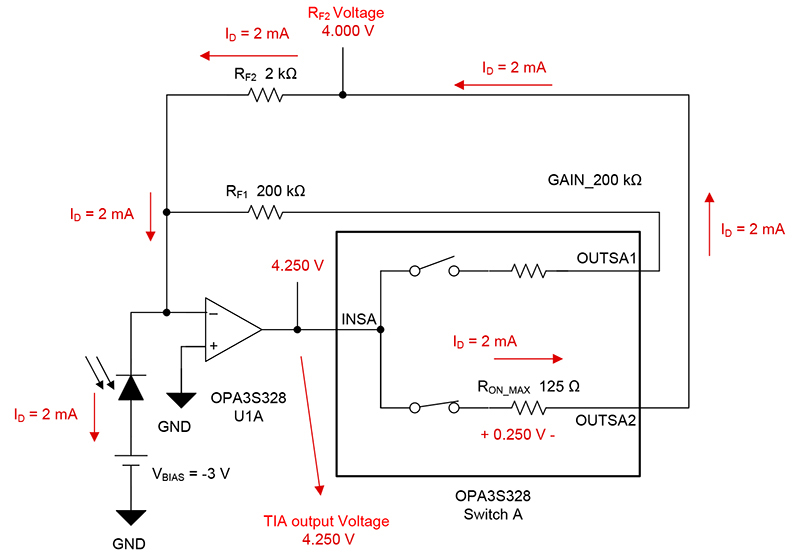
On the programmable TIA, the voltage error across RON can be significant at the higher photodiode currents.
Figure 3 shows the calculation of the TIA output accounting for the RON voltage drop. In this example, the circuit is powered with a +5-V supply and uses a feedback resistor where RF2 = 2 kΩ, for a maximum photodiode current of 2 mA and a target TIA output of +4 V. The voltage drop across RON is 250 mV, however, and the TIA output has a significant error.

Figure 3: Switch RON and TIA output error
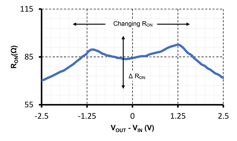
The RON will produce DC gain errors and distortion on the TIA. These gain errors are substantial at lower feedback resistor values. Furthermore, the RON changes with temperature and the switch voltage, producing gain error drift, nonlinearity and distortion. Figure 4 shows the change of RON vs. the voltage difference across the switch.

Figure 4: Switch RON vs. switch voltage
Switch Kelvin sense connections
One way to virtually eliminate or significantly reduce the gain and non-linearity errors due to the switch series resistance is to build a multiplexer using the second integrated switch of the OPA3S328. The multiplexer input senses the TIA output connection for the selected gain right at the RF feedback resistor terminal. The second amplifier stage is configured in a high-impedance noninverting configuration, buffering the multiplexer and providing an accurate Kelvin sense connection of the TIA output for each gain. Since the input bias current of the operational amplifier is minimal, less than 10 pA, the voltage drop across the switch OUTSB2 RON is negligible.
Figure 5 shows the OPA3S328 circuit using switch B in a 3-to-1 matrix configuration to build the Kelvin sense connection multiplexer, buffered with a second-stage amplifier.

Figure 5: Switch Kelvin-sense connections and high impedance buffer
The Kelvin sense connections eliminate the gain error, drift and nonlinearity because of the switch RON through the high impedance second-stage amplifier. It is also possible to configure the second stage in a noninverting gain configuration, adding flexibility for higher gains while maintaining circuit bandwidth.
Conclusion
The OPA3S328 dual operational amplifier offers low-input bias current, high DC precision performance, low noise and high bandwidth, making it a good fit for TIA applications. The device incorporates two sets of low-leakage and low-capacitance analog switches useful for the configuration of PGAs in an integrated solution. The OPA3S328 programmable TIA, using analog switches and a Kelvin sense circuit topology, can help eliminate gain error, gain error drift and nonlinearity given the switch RON.
The next installment of this series will discuss how to achieve microvoltage-level precision in thermocouple and thermopile applications.
Additional resources


