While no one can argue about the progress made on complementary metal-oxide semiconductor (CMOS) and junction field-effect transistor (JFET) designs for operational amplifiers (op amps), bipolar op amps have some serious advantages when it comes to addressing strict accuracy requirements and efficiency. Recent bipolar op amps such as TI’s OPA2206 can achieve an impressive 2 μV of offset voltage and 0.04 μV/°C of offset drift, rivaling some of the best chopper-stabilized (zero-drift) op amps.
Despite their popularity for DC precision and low noise, bipolar op amps suffer from high input bias, a relatively low input impedance and high-current noise density, making them prohibitive in application circuits interfacing with high impedances such as biological sensors in medical instrumentation and life sciences.
However, with the implementation of tightly matched super beta transistors and TI’s proprietary e-trimTM technology, modern bipolar op amps offer a very low offset voltage and offset drift. The addition of e-trim technology provides better long-term stability, a key priority in industrial applications. Super beta transistors have very low input bias current as well as low-current noise density. As such, recently released devices such as the OPA2205 exhibit a lower input bias current when compared to a state-of-the-art CMOS.

Industry-leading offset voltage and ultra-low drift
 |
Improve system efficiency and strengthen system protection with the OPA2205 and OPA2206 precision bipolar op amps. |

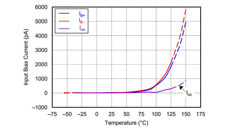
Take for example an OPAx192 precision CMOS op amp. While this device’s input bias current is only 20 pA max at 25°C, that current increases to 5 nA at 125°C. The OPA2205 super beta bipolar op amp with e-trim technology, on the other hand, has an input bias current of only ±1.2 nA at 125°C. That’s quite an improvement in applications with extreme temperature requirements. Figure 1 shows the input bias current versus temperature of an OPAx192. Figure 2 shows the input bias current of the OPA2205.

Figure 1: An OPAx192’s input bias current over temperature

Figure 2: The OPA2205’s input bias current over temperature
Generally, Equation 1 expresses current noise density as:
 (1)
(1)
where q is the charge of an electron, 1.6E-19, and Ib is the uncanceled input bias current.
It is possible to derive the input impedance using the half-circuit concept and the π model with Equation 2:
 (2)
(2)
Which then simplifies to Equation 3:
 (3)
(3)
Addressing efficiency
When computing the total error budget, you must account for offset voltage, offset voltage drift, input bias current and noise. Depending on the source impedance, you may have to carefully consider the input current noise versus the voltage noise.
One of the problems with low-noise op amps is that they tend to consume quite a bit of current. That’s because noise is inversely proportional to quiescent current. To put things in context, a precision, low-power CMOS op amp with a quiescent current of 200 μA would generate about 15 nV/√Hz of voltage noise density. In contrast, a bipolar op amp like the OPA2205 generates about 7 nV/√Hz for a mere 250 μA.
In applications with a narrow bandwidth or slow-moving signals such as temperature monitoring and control, or high-channel-count circuits such as programmable logic controllers and analog input modules, you must also account for the low frequency noise (1/f component) when considering noise requirements. In such cases, bipolar op amps prevail, since the 1/f corner is much lower when compared to CMOS- or JFET-input op amps. You can usually expect an order of magnitude lower 1/f when designing with a bipolar op amp.
Do zero-drift op amps eliminate the 1/f component?
Zero-drift op amps are great for 1/f reduction – elimination in chopper-stabilized op amps or √2 x Vnoise_bb in auto-zero op amps – but their low-frequency broadband noise is much higher than in bipolar op amps for a given IQ. Their input bias currents do tend to be much higher despite their CMOS architecture, however, and require impedance matching. And while zero-drift op amps do offer unprecedented low levels of offset voltage and drift, they are not as efficient as bipolar op amps. In other words, for the same amount of quiescent current, bipolar op amps provide a wider bandwidth and a lower noise floor.
In designs where you need efficiency, noise immunity and precision, the modern bipolar topologies I’ve discussed in this article are, in my opinion, superior to any other process technology.
Additional resources:


 (2)
(2) (3)
(3)