Not all amplifier designs are created equal, and it’s important to be familiar with common specifications and understand certain concepts when designing with high-speed amplifiers. In the context of this article, high-speed amplifiers refer to operational amplifiers (op amps) with a gain bandwidth product (GBW) greater than or equal to 50 MHz, but these concepts can apply to lower-speed devices as well. Here are some common questions designers have when using high-speed amplifiers.
Q: Why do some high-speed op amps have a minimum gain specification?
A: Decompensated op amps have a closed-loop minimum gain stable specification, but offer a wider GBW and lower noise – for the same current consumption – as their unity-gain-stable counterparts.
“Decompensated” simply means that there is a second pole above 0 dB placed in the Aol (open-loop gain) response curve. This second pole also dictates the minimum gain required to ensure the amplifier’s stability. Think of the Aol curve being “shifted up,” as shown in Figure 1. The increased Aol results in a wider bandwidth.

Figure 1: Open-loop gain response curve for decompensated amplifiers
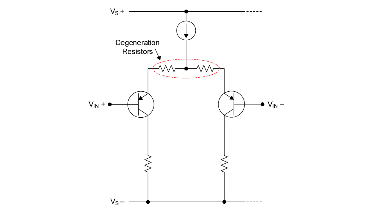
Reducing the size of the degeneration resistors in the input pair of the amplifier increases Aol, as illustrated in Figure 2. Smaller degeneration resistors also help reduce amplifier noise.

Figure 2: Degeneration resistors in an op amp
The OPA858 and OPA859 are two examples of a decompensated and unity-gain-stable amplifier, respectively. For the same current consumption, the OPA858 has wider bandwidth and lower noise, as shown in Table 1.
|
|
OPA858
(Decompensated)
|
OPA859
(Unity gain stable)
|
|
Quiescent current (IQ)
|
20.5 mA
|
20.5 mA
|
|
Gain Bandwidth (GBW)
|
5,500 MHz
|
900 MHz
|
|
Voltage noise (Vn)
|
2.5 nV/√Hz
|
3.3 nV/√Hz
|
|
Slew rate
|
2,000 V/μs
|
1,150 V/μs
|
|
Minimum gain (Acl)
|
7 V/V
|
1 V/V
|
Table 1: Comparing decompensated and unity-gain-stable amplifiers
In addition to increased bandwidth and lower noise, the decompensated architecture also enables a higher slew rate. Overall, the minimum gain specification offers a trade-off in performance that you can take advantage of if you can forego unity gain and meet the minimum gain requirement. Examples of applications where it’s possible to easily meet the minimum gain specification include current-sensing circuits that measure a voltage across a shunt resistor, gain stages in a signal chain and transimpedance circuits.
Q: What are current feedback amplifiers?
A: Current feedback amplifiers are op amps that feed back a portion of the output signal as current in order to control the amplifier. Current feedback amplifiers differ from voltage feedback amplifiers that rely on feedback in the form of a voltage. Most designers are familiar with voltage feedback architectures because they are more common and emphasized in most electronics curriculums.
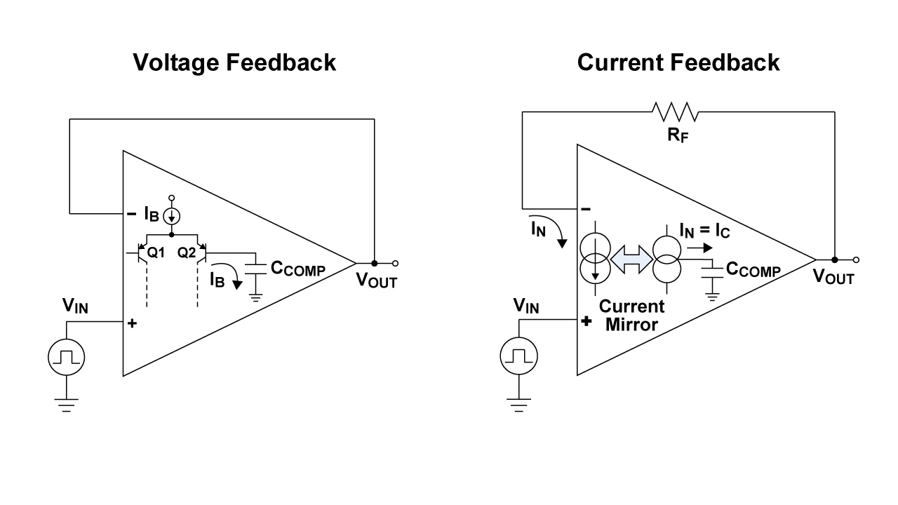
Figure 3 offers a basic input-stage comparison of voltage and current feedback amplifier architectures, where the voltage feedback amplifier is modeled as a voltage-controlled voltage source and the current feedback amplifier is modeled as a current-controlled voltage source.

Figure 3: Comparing voltage and current feedback op amp architectures
Both architectures are still used as error amplifiers in a negative feedback circuit, but the type of feedback they require is what differs. You can use either amplifier type in inverting and noninverting gain configurations, for instance. One distinct advantage of the current feedback architecture is that the bandwidth is not dependent on the gain. In the voltage feedback architecture, however, as the gain increases, the bandwidth decreases, as shown in Equation 1:

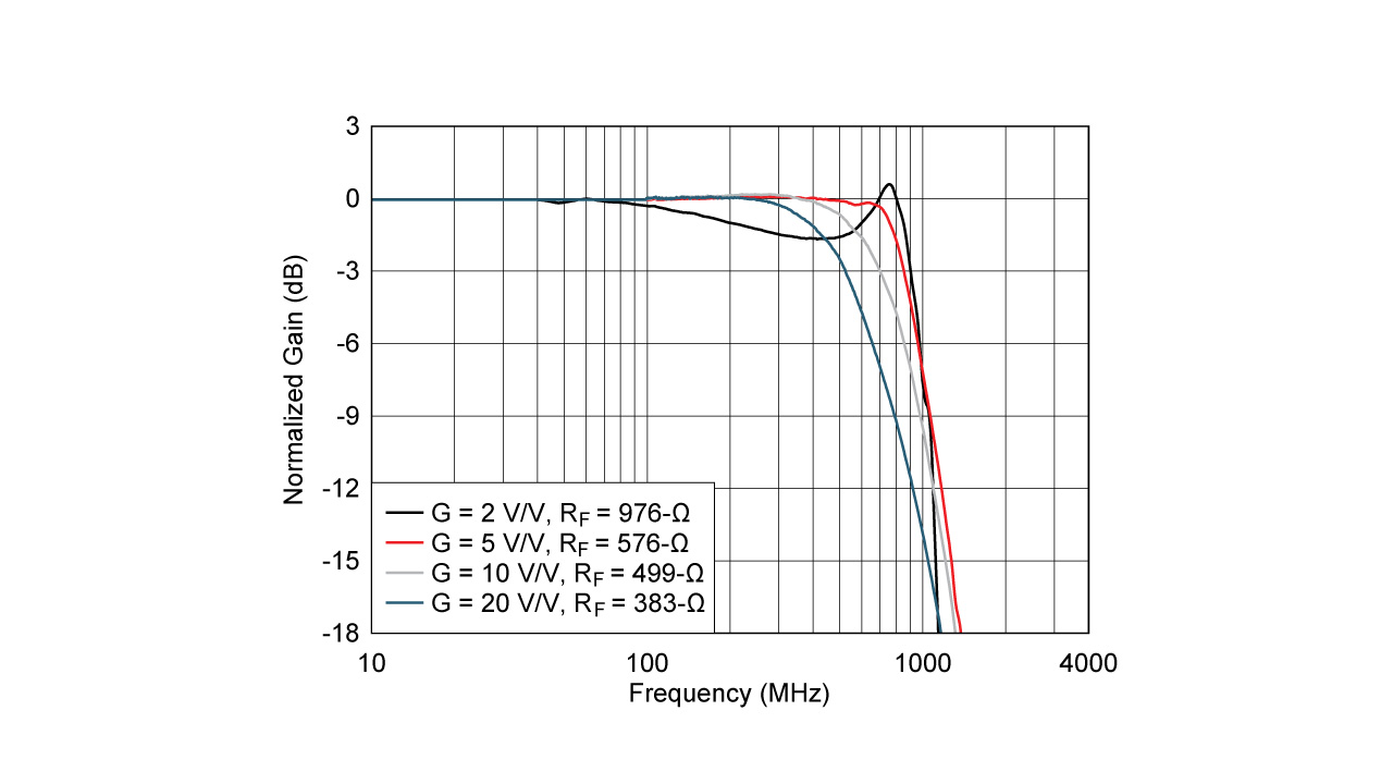
In the current feedback architecture the bandwidth remains nearly constant regardless of the gain, as shown in Figure 4. This graph appears in the THS3491 data sheet.

Figure 4: Gain and bandwidth relationship of a current feedback op amp
Table 2 compares some of the main differences between voltage and current feedback amplifiers.
|
|
Voltage feedback amplifier
|
Current feedback amplifier
|
|
Bandwidth
|
Bandwidth varies with gain
|
Almost constant bandwidth over gain
|
|
DC accuracy
|
Good
|
Poor
|
|
Output swing
|
Many rail-to-rail output options
|
Larger headroom needed for output
|
|
Distortion
|
Better low-frequency distortion
|
Better high-frequency distortion
|
|
Slew rate
|
Limited slew rate
|
Very high slew rate facilitating high full-power bandwidth
|
|
Gain stability
|
Restriction on the minimum stable gain for decompensated amplifiers
|
Stable across gains if feedback transimpedance remains constant
|
|
Noise
|
Low input-referred voltage and current noise
|
Higher input-referred current noise (unequal for inverting and noninverting inputs)
|
|
Typical applications
|
Applications requiring DC precision
Pulse-oriented applications
High-speed and precise analog-to-digital converter (ADC) interfaces
Transimpedance applications
|
Digital-to-analog converter interfaces
Output drivers
High-speed ADC interfaces
Sallen-Key filters
|
Table 2: Comparing voltage feedback and current feedback amplifier applications
Note that current feedback amplifiers are not meant to operate without a resistor in the feedback path. A current feedback amplifier data sheet will suggest specified values for RF; these values are important because the value of RF dictates the compensation of the amplifier, even in unity gain. Like Figure 4, Table 3 is from the THS3491 data sheet.

Table 3: Example of recommended values for RF from the THS3491 data sheet
For more details about the differences between these two architectures, check out Understanding Voltage Feedback and Current Feedback Amplifiers. You can also learn more about current feedback architectures by watching the TI Precision Labs online training videos.
Q: Why does my high-speed amplifier oscillate when I put it on a breadboard?
A: Generally speaking, it’s likely that the inductance of the package leads as well as the breadboard’s capacitance and inductance are causing your high-speed amplifier to oscillate. Similarly, when designing with high-speed op amps, it’s important to minimize capacitance and inductance on printed circuit boards (PCBs). Even devices on the lower end of the high-speed amplifier GBW spectrum, like the 50-MHz OPA607, require these types of board-level design considerations.
Here are some ways you can optimize your high-speed layout design:
- Minimize trace length. Minimizing the trace length reduces additional capacitance and inductance.
- Use solid ground planes. Solid ground planes are generally a better choice than a hashed plane for high-speed designs.
- Cut out ground planes under signal traces. Removing the ground plane metal underneath the input and outputs of the device helps reduce parasitic capacitance on sensitive nodes.
- Minimize vias on signal paths. Vias increase inductance and can cause signal fidelity issues at frequencies greater than 100 MHz. To mitigate signal fidelity, route critical signals on the same layer as the amplifier in order to eliminate any vias.
- Optimize return current paths. Signal trace layout design should minimize the overall signal-loop area and thus minimize the inductance.
- Properly place and route bypass capacitors. Place bypass capacitors as close as possible to the amplifier on the same layer of the board. Use wider traces and route vias into the bypass capacitors and then to the amplifier – not between the capacitors and the amplifier.
- Properly place resistors. Place gain-setting, feedback and series-output resistors close to the device pins to minimize board parasitics.
When evaluating the performance of high-speed op amps, it’s best to use the designated evaluation module for a particular device. These boards demonstrate good high-speed board layout design and use SMA connectors to maintain a high-fidelity and impedance-controlled signal path. For more details on high-speed board layout practices, you can read High Speed PCB Layout Techniques.
Overall, high-speed op amps operate much like their lower-speed counterparts. By considering just a few design nuances, you can take advantage of all of the speed and performance benefits that they offer for your system. Which of these questions were most relevant to you? Leave a comment below.


