Other Parts Discussed in Post: TLV9004 (Note: Paul Goedeke co-authored this technical article.)
Quad package operational amplifiers (op amps) offer good value in terms of cost per channel and can help save space on a printed circuit board (PCB) during layout. It’s common to use a multichannel op amp in applications such as three-phase motors and multiple LED strings, which sense multiple currents. However, using a quad op amp can introduce some complexities. In this article, I’ll discuss some PCB layout considerations when using quad op amps.
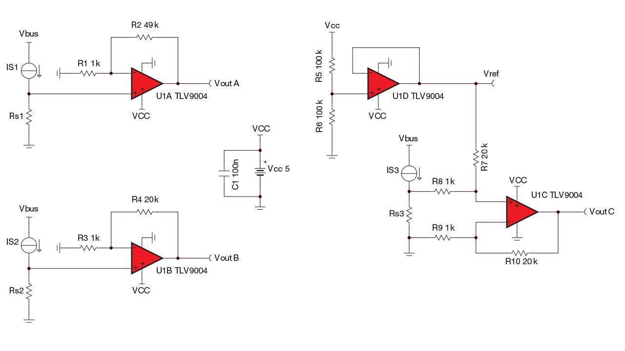
Figure 1 shows an example schematic, with generic current sources IS1, IS2 and IS3 representing the measured currents. Channels A and B are both unidirectional low-side current-sense circuits, each with their own gains. Channel D is a buffer for a reference voltage used by channel C in a bidirectional current-sense circuit.

Figure 1: Multicurrent sensing schematic example
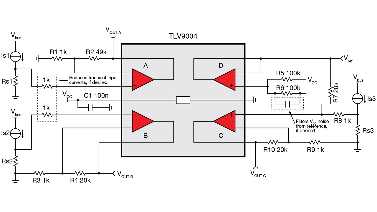
Figure 2 shows the same schematic but arranged around a shared, quad amplifier package. Careful layout is required to avoid turning floorplanning compromises into liabilities that impact circuit performance. Optimal placement for all channels may be difficult given the number of components and the need to place the sense resistors close to the device.

Figure 2: Example schematic shown around a shared amplifier package
Designs that measure multiple currents are more susceptible to parasitic inductances because of the amount of current flowing through the ground net. For example, a long, thin trace between the ground nodes of two components on a PCB will have a high parasitic inductance. High-frequency signals (such as noise or large transients) can turn small parasitic inductances into large impedances, which creates a potential difference between the ground nodes.
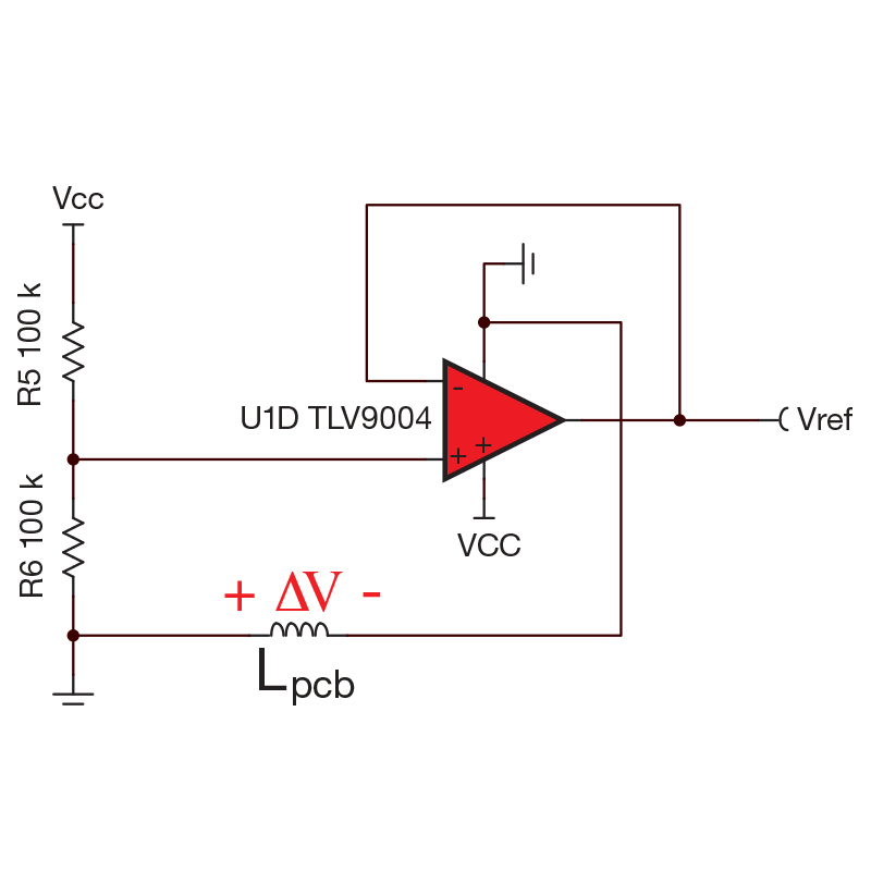
You can see this effect in Figure 3, which shows the channel D buffer circuit from Figure 1. A long trace between the ground node of R6 (shown in Figures 1 and 2) and the ground node of the op amp causes the parasitic inductance, shown as Lpcb. A transient creates a voltage delta across Lpcb, which means that the op amp and R6 are referenced to different potentials. For more information on PCB parasitic inductance, see the “Analog Engineer’s Pocket Reference” and “Analog Engineer’s Calculator.”

Figure 3: Parasitic inductance from PCB trace
To understand why these parasitic inductances can cause an issue, remember that the voltage across an inductor is determined by Equation 1, and that the current through an inductor cannot change instantaneously:
 (1)
(1)
Therefore, when a current transient occurs, the inductance of the trace fights the change in current and develops a voltage potential known as ground bounce. In some cases, ground bounce may cause device damage by violating the data-sheet’s absolute maximum limits for voltage and current.
In the case of the reference circuit on channel D (shown in Figure 3), ground bounce impacts the performance of the circuit by shifting the buffered voltage created by the R5 and R6 resistor divider. Channel C uses that value as a reference point, so any change in the reference impacts its output as well.
To reduce the effects of ground bounce and maintain system performance, keep these PCB layout considerations in mind:
- Use Kelvin connections to the sense resistors to help eliminate the impact of parasitic trace and pad resistance in the measurement. Make sure that the sense traces are routed to the inside of the sense resistor footprint.
- Try to keep the trace lengths to each sense resistor as short as possible and use balanced trace lengths for both Kelvin connections. If possible, move the sense resistors to achieve a better layout.
- During layout, carefully consider the return current path:
- Use ground planes to create a low-impedance return path.
- When using a ground plane, make sure that no islands are created or that current is forced to take a long path around other traces. If necessary, connect with vias to a ground plane on another layer.
- Keep a short path between the ground nodes of filtering and decoupling components and the ground node of the op amp.
In general, follow the best practices for current-sensing circuit layouts as discussed in the technical article, “How to lay out a PCB for high-performance, low-side current-sensing designs.” For general PCB layout considerations for op amps, read “The basics: How to lay out a PCB for an op amp.”
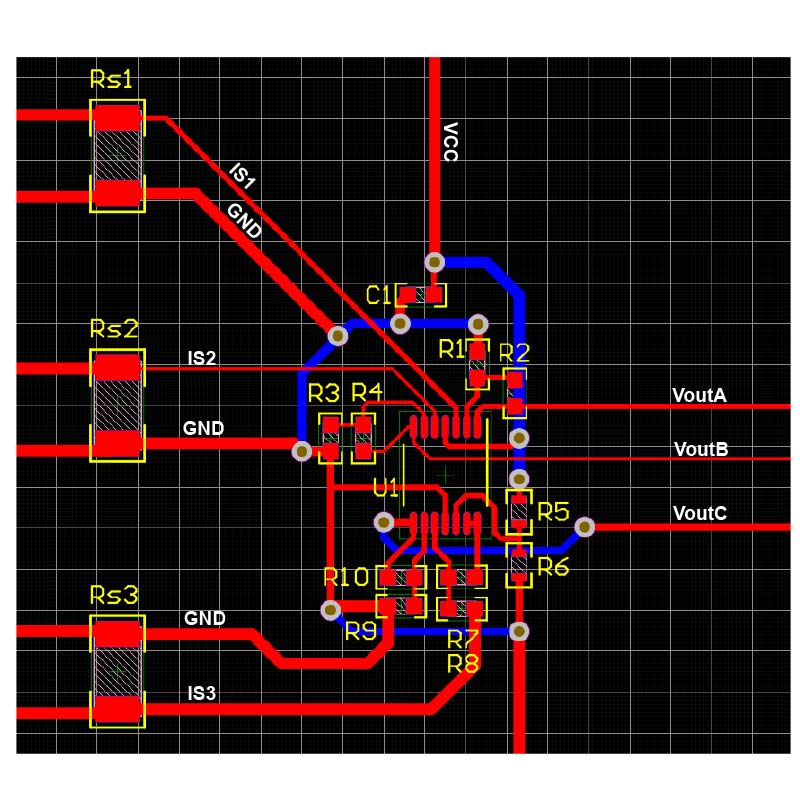
Let’s look at a couple of example circuit layouts using the schematic in Figure 1 and the Texas Instruments (TI) TLV9004 op amp in a 14-pin thin-shrink small-outline package. Figure 4 shows a nonideal PCB layout.

Figure 4: Example of a poor quad layout
Here are the major concerns with this layout:
- The return path is made up of long thin traces.
- No ground planes are used.
- The sense resistors are far from the op amp and are not Kelvin connected.
- The connections to the sense resistors have long, unequal trace lengths and differing widths.
- The decoupling capacitor, C1, is far from the op amp’s VCC pin.
- The supply voltage doesn’t pass through the decoupling capacitor before connecting to the op amp.
- There are many more vias than the circuit requires, adding inductance and complexity.
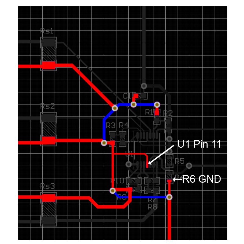
Figure 5 shows the same nonideal layout but with the ground net highlighted. Notice the long trace between the negative supply pin of the op amp and the ground of R6 (as indicated by the white arrows). This is the exact scenario shown in Figure 3.

Figure 5: Example of a nonideal quad layout with the ground net highlighted
Figure 6 shows a well-designed PCB layout for this particular circuit. This new layout is much more compact and addresses the major concerns highlighted in the nonideal layout.

Figure 6: Well-designed layout for multiple current-sensing circuits
Some notable changes:
- The components are placed close together to keep trace lengths short, reducing the susceptibility of noise coupling onto the traces.
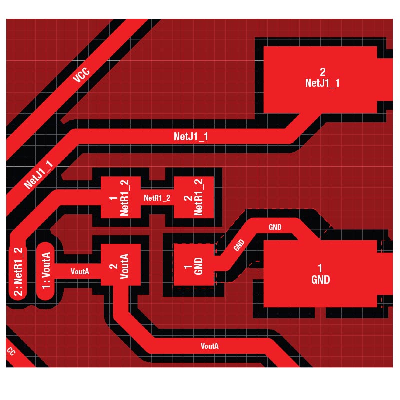
- Sense resistors are now close to the other components and use well-implemented Kelvin connections, as shown in Figure 7.
- A ground plane provides a low-impedance return path.
- The decoupling capacitor is placed as close to the op-amp supply pin as possible and routed such that the VCC trace must pass through the capacitor before connecting to the op amp.

Figure 7: Kelvin connection detail
Using a quad package amplifier is often a good decision for a circuit design because it can help save cost and space on a PCB. Using the tips discussed above and the TI TLV9004 op amp, your quad amplifier circuit design can be successful. The 1-MHz TLV9004 has built-in electromagnetic interference and radio-frequency interference filters that can help improve a circuit’s resilience to interference. This device comes in package options ranging from an industry-standard 8.65-mm-by-3.91-mm small-outline integrated circuit package to an ultra-compact 2.0-mm-by-2.0-mm super-thin quad-flat no-lead package, making it useful for many types of applications.
Additional resources


