Galvanic isolation is a necessary form of protection for all electronics that interface with humans or other circuits against possible high-voltage events ranging from tens of volts to kilovolts. Isolation as a form of protection requires that communication between two circuits occurs through an insulation or isolation barrier, which prevents current from directly flowing between the circuits.
Over the past several decades, the technology used to isolate circuits has moved from optical-based to silicon-based – but how are these technologies really different?
How does an optocoupler work?
An optocoupler, as shown in Figure 1, consists of an input LED, a receiving photodetector and an output driver. The driver circuit and LED circuits are typically built using complementary metal-oxide semiconductor (CMOS) technology, with the insulation or isolation barrier usually consisting of molding compound. Both the input and output of an optocoupler isolator require separate voltage supplies connected through the anode and collector pins, and separate grounds typically connected at the cathode and emitter pins, in order to maintain signal isolation between the input and output.

Figure 1: Optocoupler with pinout diagram
Communication within an optocoupler occurs when an applied CMOS logic input generates an input-side current, which then creates a proportional LED output for transmission through the molding compound barrier to the receiving photodetector and output.
The isolation performance of an optocoupler is determined by a combination of the LED, the molding compound used between the input and output, and the distance through the molding compound. Because the molding compound is a key contributor to isolation barrier strength, its quality plays a significant role in optocoupler lifetime, reliability and performance.
Standards bodies including Underwriters Laboratories (UL) and Verband der Elektrotechnik (VDE) determine optocoupler ratings, and those ratings specifically define the “distance through insulation” to accommodate molding compound variations during manufacture, along with partial discharge tests to identify molding compound defects that could compromise isolation performance under stress. Optocoupler standards have not historically included lifetime reliability performance data or high-voltage stress testing for sustained applied high voltages, and thus their sustained long-term performance and reliability can vary significantly.
How does a silicon-based isolator work?
Silicon-based isolation technology is based on CMOS technology, and consists of two separate integrated circuit (IC) chips – an input circuit and an output circuit – connected through bond-wires to enable data transfer, as shown in Figure 2.

Figure 2: Cross section of digital isolator construction
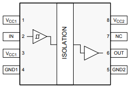
Both the input and output sides of the digital isolator, as shown in Figure 3, require separate voltage supplies (VCC1, VCC2) and separate grounds (GND1, GND2) to maintain signal isolation between the input and output.
Communication within a digital isolator occurs when applying a transistor-transistor logic or CMOS logic input to the digital input. The input signal is digitally translated into the frequency domain and then passed through a high-voltage capacitive barrier and across the connecting bond-wire to the receiving-side IC.

Figure 3: Digital isolator with pinout diagram
The insulator of a digital isolator circuit can be either a single or double silicon dioxide (SiO2) capacitive barrier, which can withstand extremely high voltages by design. Because the insulation barrier is constructed of high dielectric strength material (see Table 1) and is manufactured in a closely controlled wafer fab instead of an assembly line, part-to-part variation is unlikely, and the key contributors to isolation performance are the isolation technology and design. The white paper, "Enabling high voltage signal isolation quality and reliability," explores how this manufacturing process provides reliability, shock protection and reinforced isolation equivalent to two levels of basic isolation in a single package.
|
Insulator Materials
|
Dielectric Strength
|
|
Air
|
~1 Vrms/μm
|
|
Epoxies
|
~20 Vrms/μm
|
|
Silica-filled mold compounds
|
~100 Vrms/μm
|
|
Polyimide
|
~300Vrms/μm
|
|
SiO2
|
~500 Vrms/μm
|
Table 1: Comparison of dielectrics
The isolation ratings of silicon-based digital isolators are determined by a series of high-voltage tests defined through industry standards bodies such as UL, the International Electrotechnical Commission and VDE. The tests are the same as those for determining optocoupler ratings, as shown in Table 2, with additional high-voltage testing and material rating requirements. Because of the additional test conditions for high-voltage robustness and reliability, it is possible to publish lifetime reliability data.
|
|
Topic
|
VDE 0884-11 Capacitive & Magnetic Digital Isolators
|
IEC 60747-5-5 Optocouplers
|
|
|
|
Basic isolation
|
Reinforced isolation
|
Reinforced isolation only
|
|
1
|
Max surge isolation voltage VIOSM
|
Test voltage = VIOSM x 1.3
|
Test voltage VIOSM x 1.6
|
Min 10 kV
|
|
Min. 10 kV
|
|
2
|
Partial discharge test voltage, VPD(M)
|
1.5 x VIORM
|
1.875 x VIORM
|
1.875 x VIORM
|
|
3
|
Working voltage, VIORM
|
Based on TDDB analysis
|
Based on TDDB analysis
|
Based on PD test
|
|
4
|
Min. rated lifetime
|
20 years x 1.3 (security factor)
|
20 years x 1.875 (security factor
|
Not defined
|
|
5
|
Failure rate over lifetime
|
1000 ppm
|
1 ppm
|
Not defined
|
|
6
|
Allowed isolation materials
|
SiO2 and thin film polymer
|
SiO2 and thin film polymer
|
Not limited
|
Table 2: Comparison of optocoupler test conditions/digital isolator tests
You should now have some insight into differences between optical isolation and silicon-based isolation performance, and the role of materials, manufacturing and even standards testing. While both optocoupler and silicon-based isolators are proven means of circuit protection, the real challenge in identifying the best isolation solution for your design will depend on your design objectives: reliability, lifetime and performance of the isolator all play a role in the right technology choice.
Additional resources:


